Choosing the Right PCB Assembly Equipment: A Cost-Effective Comparison for Engineers
Choosing the Right PCB Assembly Equipment: A Cost-Effective Comparison for Engineers table { border-collapse: collapse; width: 100%; margin: 20px 0; } th, td { border: 1px solid #ddd; padding: 8px; } ...
Introduction
In the rapidly evolving field of electronics, selecting the right equipment for PCB assembly is critical for ensuring quality, efficiency, and cost-effectiveness. Engineers are tasked with making informed decisions that will affect the overall performance and reliability of the electronic products. This article aims to provide a comprehensive guide to choosing the right PCB assembly equipment by examining PCB layout rules, stackup design, signal integrity, and manufacturing considerations. With a focus on cost-effective solutions, this guide will help engineers navigate the complexities of PCB design and assembly.
Technical Overview
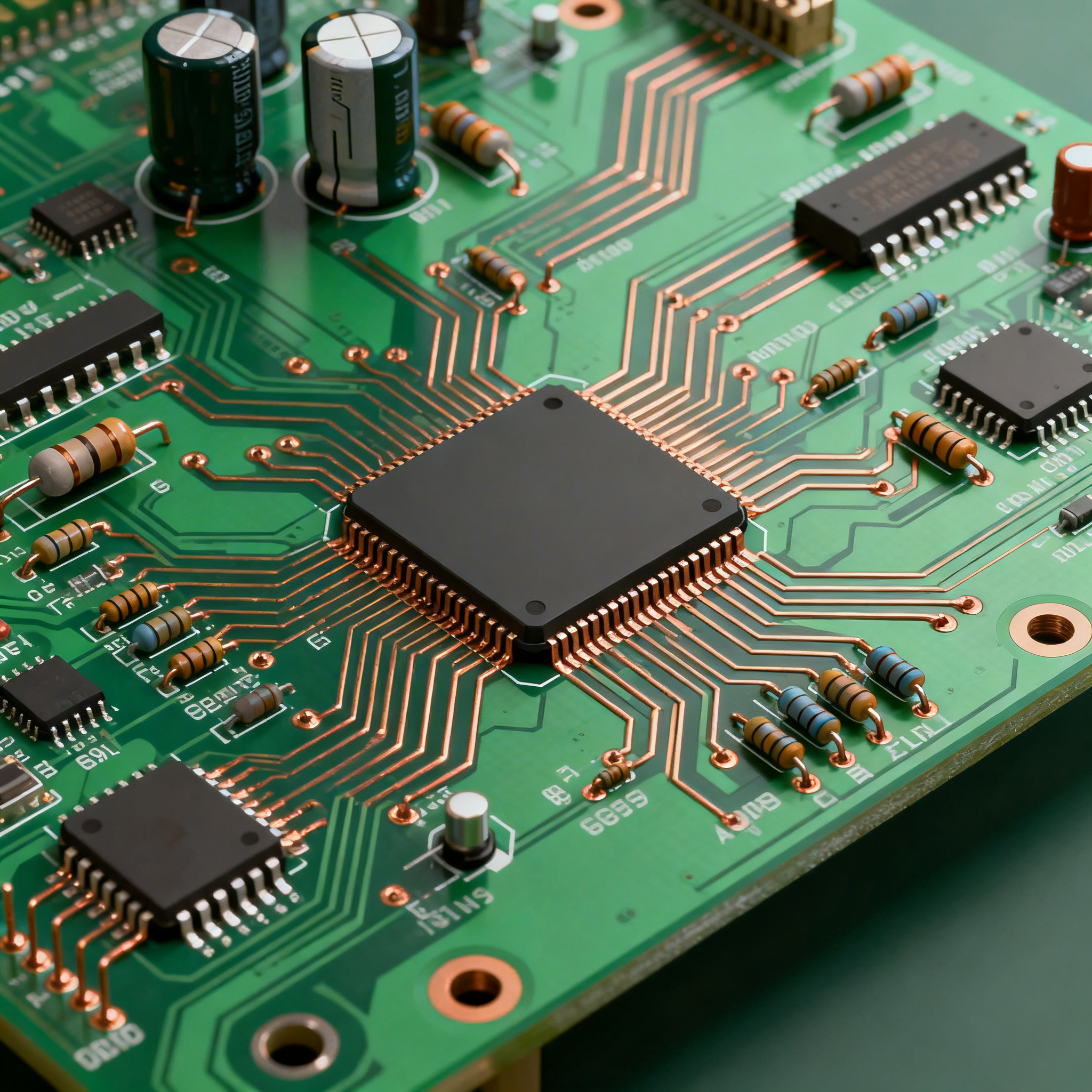
Printed Circuit Boards (PCBs) are the backbone of electronic devices, providing the mechanical support and electrical connections for components. The design and assembly of PCBs involve intricate processes that require precision and adherence to industry standards. Core concepts such as trace width, spacing, and via sizes are crucial for ensuring signal integrity and reducing interference. Understanding the architecture and principles of PCB design, including stackup configurations and material properties, is essential for optimizing performance and manufacturability.
Detailed Specifications
When it comes to PCB design, certain specifications are paramount. These specifications determine the electrical performance, manufacturability, and cost-effectiveness of the board. Engineers must pay close attention to design rules such as trace width, spacing, and via sizes, as well as stackup options and material properties. These factors influence signal integrity, thermal management, and the overall reliability of the PCB.
| Design Parameter | Minimum Value | Recommended Value |
|---|---|---|
| Trace Width | 0.15 mm | 0.20 mm |
| Trace Spacing | 0.15 mm | 0.20 mm |
| Via Diameter | 0.30 mm | 0.40 mm |
| Via Hole Size | 0.15 mm | 0.20 mm |
| Pad Diameter | 0.60 mm | 0.70 mm |
| Annular Ring | 0.05 mm | 0.10 mm |
| Clearance to Edge | 0.50 mm | 1.00 mm |
| Solder Mask Clearance | 0.05 mm | 0.10 mm |
| Silkscreen Line Width | 0.10 mm | 0.15 mm |
| Component Clearance | 0.50 mm | 1.00 mm |
Key Takeaways from the Specifications
These design rules are fundamental to ensuring the functionality and reliability of PCBs. For instance, maintaining appropriate trace width and spacing is crucial for minimizing potential crosstalk and maintaining signal integrity. Via sizes and clearances affect the mechanical stability and electrical performance of the board. Engineers should adhere to these recommended values to optimize the manufacturability and performance of the PCB, considering factors such as current carrying capacity and thermal dissipation.
| Stackup Configuration | Number of Layers | Applications |
|---|---|---|
| Single Layer | 1 | Simple, Low-Cost Circuits |
| Double Layer | 2 | Consumer Electronics |
| Four Layer | 4 | Complex Circuits, RF Applications |
| Six Layer | 6 | High-Speed Digital |
| Eight Layer | 8 | Advanced Computing |
| Ten Layer | 10 | High-Density Interconnects (HDI) |
| Twelve Layer | 12 | Advanced Telecom |
Practical Implications
The choice of layer stackup is pivotal in addressing the electrical and mechanical requirements of a PCB. For instance, a four-layer board offers better signal integrity and power distribution compared to a double-layer board, making it suitable for RF applications. As complexity increases, additional layers allow for more routing options, reduced electromagnetic interference (EMI), and improved thermal management. Engineers must carefully consider the application requirements and cost implications when selecting the appropriate stackup configuration.
| Material | Dielectric Constant (Dk) | Loss Tangent (Df) |
|---|---|---|
| FR-4 | 4.5 | 0.02 |
| Rogers 4350B | 3.66 | 0.0037 |
| Rogers 4003C | 3.55 | 0.0027 |
| Teflon | 2.1 | 0.0005 |
| Polyimide | 4.2 | 0.004 |
| Ceramic | 9.8 | 0.001 |
| BT Epoxy | 3.9 | 0.008 |
| Alumina | 9.4 | 0.0001 |
| PTFE | 2.2 | 0.001 |
Application Guidelines
The choice of material significantly impacts the electrical performance and thermal stability of the PCB. FR-4 is a versatile and cost-effective material commonly used in standard applications. For high-frequency applications, materials like Rogers 4350B offer lower dielectric constants and loss tangents, which are essential for minimizing signal loss. Polyimide and ceramic materials provide excellent thermal stability for high-temperature applications. Engineers should select materials based on the specific electrical, mechanical, and thermal requirements of their projects.
Design Considerations
When designing a PCB, engineers must consider various factors that influence both the performance and manufacturability of the board. Signal integrity is a critical aspect, requiring careful attention to trace impedance, return paths, and crosstalk. The choice of stackup and materials impacts thermal management and mechanical stability. Additionally, compliance with industry standards, such as those set by IPC, ensures reliability and quality. Design for manufacturability (DFM) principles should be incorporated to optimize the assembly process and reduce costs. Engineers must also consider environmental factors, such as operating temperature and humidity, which can affect the longevity and performance of the PCB.
Step-by-Step Implementation
Implementing a PCB design requires a methodical approach to ensure all aspects are covered from concept to production. Here is a step-by-step guide:
- Define Requirements: Begin by outlining the electrical, mechanical, and environmental requirements of the project. This includes determining the number of layers, material selection, and specific design constraints.
- Create the Schematic: Develop a detailed schematic using CAD software, ensuring all components are correctly placed and interconnected.
- Layout Design: Translate the schematic into a PCB layout, adhering to design rules for trace width, spacing, and via placement. Consider signal integrity and thermal management during this phase.
- Stackup Configuration: Choose the appropriate stackup based on the complexity and application of the PCB. Ensure proper layer sequencing for power and ground planes.
- Material Selection: Select materials that meet the electrical and thermal requirements, considering factors such as dielectric constant and loss tangent.
- Prototype and Testing: Fabricate a prototype for testing. Evaluate the board for electrical performance, signal integrity, and thermal behavior. Conduct necessary revisions based on test results.
- DFM Review: Perform a design for manufacturability review to identify potential production issues and optimize the design for cost-effective assembly.
- Finalize Design: Make final adjustments and prepare the design files for production. Ensure compliance with industry standards and customer requirements.
Common Issues & Solutions
During PCB design and assembly, engineers may encounter several common issues. Here are some solutions:
- Signal Integrity Problems: Use proper termination techniques, maintain consistent trace impedance, and minimize crosstalk through careful trace routing and spacing.
- Thermal Management: Implement thermal vias, use heat sinks, and select materials with appropriate thermal conductivity to manage heat dissipation.
- Manufacturing Defects: Conduct thorough DFM reviews, use automated optical inspection (AOI), and adhere to IPC standards to minimize defects.
- EMI/EMC Issues: Employ shielding techniques, maintain proper ground planes, and use filters to reduce electromagnetic interference.
- Component Placement Errors: Verify component orientations and clearances, use pick-and-place machines with high precision, and conduct visual inspections.
- Material Incompatibility: Ensure compatibility of materials with operating conditions and environmental factors to prevent failures.
Applications & Use Cases
PCBs are integral to a wide range of applications, from consumer electronics to advanced telecommunications. In consumer devices, such as smartphones and tablets, PCBs provide compact and efficient platforms for integrating various functions. In automotive and aerospace industries, PCBs are used for robust and reliable control systems. High-frequency applications, like radar and RF communication, benefit from specialized materials and stackup configurations. Each application demands specific considerations for design, material selection, and assembly processes to ensure optimal performance and reliability.
Selection & Sourcing Guide
When selecting and sourcing PCB assembly equipment, engineers should focus on factors such as equipment capabilities, cost, and compatibility with design requirements. Engaging with reputable suppliers and manufacturers, such as those listed on IC Online, can provide access to a wide range of options and expertise. It is crucial to evaluate the supplier's technical support, lead times, and quality assurance processes to ensure a successful partnership.
FAQ
- What is the importance of trace width in PCB design?
Trace width affects the current-carrying capacity and resistance of the trace, impacting signal integrity and thermal performance. - How do I choose the right layer stackup for my PCB?
Consider the complexity, signal integrity requirements, and application-specific needs to determine the appropriate stackup. - Why is material selection critical in PCB design?
Material properties, such as dielectric constant and thermal stability, influence the electrical performance and reliability of the PCB. - What are common methods for managing heat in PCBs?
Use thermal vias, heat sinks, and materials with high thermal conductivity to effectively dissipate heat. - How can I minimize EMI in my PCB design?
Implement proper grounding, use shielding techniques, and maintain optimal trace routing and spacing. - What role do IPC standards play in PCB design?
IPC standards provide guidelines for design, assembly, and quality assurance, ensuring reliability and consistency in PCBs. - How can I ensure manufacturability in my PCB design?
Incorporate DFM principles, conduct thorough reviews, and collaborate with manufacturers to optimize the design for production. - What are the benefits of using advanced materials like Rogers?
Advanced materials offer lower dielectric constants and loss tangents, improving performance in high-frequency applications. - How do I address component placement challenges?
Use precise pick-and-place equipment, verify clearances, and conduct visual inspections to ensure accurate placement. - What factors should I consider when sourcing PCB assembly equipment?
Evaluate equipment capabilities, cost-effectiveness, and supplier support to ensure alignment with project requirements.
Conclusion
Choosing the right PCB assembly equipment and design considerations is crucial for achieving optimal performance, reliability, and cost-effectiveness in electronic products. By understanding and applying PCB design rules, stackup configurations, and material properties, engineers can make informed decisions that enhance the quality and functionality of their designs. Adhering to industry standards and leveraging advanced technologies will ensure successful PCB assembly and manufacturing outcomes.