Effective PCB Testing Methods: A Troubleshooting Guide to Ensure Reliability
Effective PCB Testing Methods: A Troubleshooting Guide to Ensure Reliability Introduction In the realm of electronics, ensuring the reliability of printed circuit boards (PCBs) is paramount. PCBs serv...
Introduction
In the realm of electronics, ensuring the reliability of printed circuit boards (PCBs) is paramount. PCBs serve as the backbone of electronic devices, and their performance directly impacts the functionality and longevity of the final product. With the increasing complexity of electronic designs, effective PCB testing methods have become more critical than ever. This article delves into various PCB testing methods, exploring how careful attention to design rules, stackup options, and material properties can enhance reliability and performance.
Technical Overview
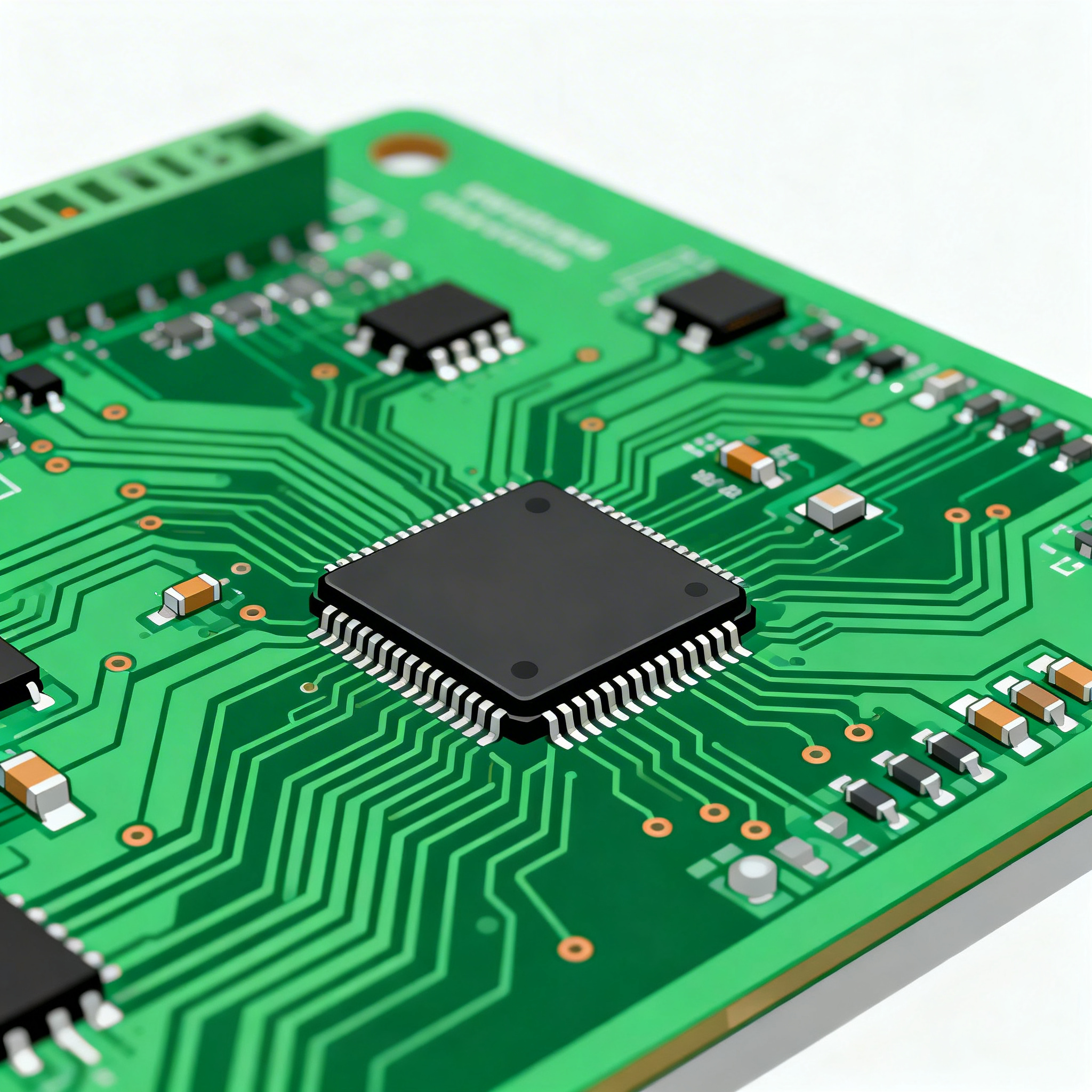
PCBs are integral to the functioning of electronic circuits, providing mechanical support and facilitating electrical connections. The core concepts of PCB design include layout rules, stackup configurations, signal integrity, and manufacturing considerations. Adhering to industry standards, such as those set by IPC, ensures quality and reliability. Understanding the architecture and principles of PCB design is crucial for both designers and manufacturers aiming to produce high-quality boards. This section provides an overview of these core concepts, setting the stage for a deeper dive into the detailed specifications and testing methods that follow.
Detailed Specifications
Specifications play a pivotal role in PCB design and testing, establishing the parameters within which a board must operate. These include trace width, spacing, via sizes, and clearances, which are critical for signal integrity and thermal performance. Understanding these specifications is essential for designers to create reliable and efficient PCBs.
| Design Rule | Minimum Value | Recommended Value |
|---|---|---|
| Trace Width | 0.15 mm | 0.25 mm |
| Trace Spacing | 0.15 mm | 0.20 mm |
| Via Diameter | 0.30 mm | 0.50 mm |
| Pad Diameter | 0.60 mm | 0.80 mm |
| Annular Ring | 0.10 mm | 0.15 mm |
| Clearance to Edge | 0.20 mm | 0.25 mm |
| Silkscreen Clearance | 0.10 mm | 0.15 mm |
| Solder Mask Clearance | 0.05 mm | 0.10 mm |
| Aspect Ratio | 6:1 | 8:1 |
| Drill to Copper | 0.20 mm | 0.30 mm |
| Board Thickness | 0.8 mm | 1.6 mm |
Key Takeaways from the Specifications
The specifications outlined in the table are crucial for ensuring the electrical and mechanical integrity of PCBs. Trace width and spacing directly affect current carrying capacity and signal integrity. Adequate via sizes and pad diameters are essential for reliable soldering and mechanical stability. The recommended values provide a buffer to accommodate manufacturing tolerances and environmental variations. Designers must carefully consider these specifications to prevent issues like short circuits, signal loss, and mechanical failures.
| Layer Configuration | Signal Layers | Power/Ground Layers |
|---|---|---|
| 2-Layer | 2 | 0 |
| 4-Layer | 2 | 2 |
| 6-Layer | 4 | 2 |
| 8-Layer | 6 | 2 |
| 10-Layer | 8 | 2 |
| 12-Layer | 8 | 4 |
| 14-Layer | 10 | 4 |
| 16-Layer | 12 | 4 |
Practical Implications
The choice of layer stackup is vital for accommodating complex circuitry, ensuring signal integrity, and minimizing electromagnetic interference (EMI). Higher layer counts allow for more signal routing and dedicated power/ground planes, which improve performance and reduce crosstalk. However, they also increase manufacturing complexity and cost. Designers must balance these factors based on application requirements and budget constraints, ensuring that the chosen stackup meets both functional and economic needs.
| Material | Dielectric Constant (Dk) | Loss Tangent (Df) |
|---|---|---|
| FR-4 | 4.2 | 0.020 |
| Rogers 4350B | 3.48 | 0.0037 |
| Rogers 4003C | 3.55 | 0.0027 |
| Isola FR408 | 3.75 | 0.009 |
| Nelco N4000-13 | 3.7 | 0.008 |
| Arlon 85N | 3.5 | 0.004 |
| Megtron 6 | 3.6 | 0.002 |
| Panasonic R-1755 | 4.0 | 0.016 |
| Getek | 4.0 | 0.005 |
| Duroid 5880 | 2.20 | 0.0009 |
Application Guidelines
Material properties such as dielectric constant and loss tangent significantly influence a PCB's performance, especially in high-frequency applications. FR-4 is a versatile and cost-effective choice for general use, while materials like Rogers and Megtron offer superior performance for RF and microwave applications due to their lower loss tangent. Selecting the right material involves considering factors like operating frequency, environmental conditions, and cost constraints. Understanding these properties helps designers choose materials that align with the technical and economic requirements of their projects.
Design Considerations
Designing a PCB involves a myriad of considerations that ensure optimal performance and manufacturability. From selecting the right materials and stackup configurations to adhering to design rules and signal integrity principles, each factor plays a critical role in the success of the final product. Proper thermal management, EMI control, and mechanical stability are also crucial. Designers must balance these elements while considering cost and production capabilities. Tools like CAD software and simulation programs aid in visualizing and validating the design before manufacturing, reducing the risk of errors and rework.
Step-by-Step Implementation
Implementing an effective PCB design involves several key steps:
- Define Requirements: Clearly outline the electrical, mechanical, and environmental requirements of the PCB.
- Select Materials: Choose appropriate materials based on the application's frequency, thermal, and mechanical needs.
- Design Schematic: Create a detailed schematic capturing all components and connections.
- Layout Design: Translate the schematic into a PCB layout, adhering to design rules and optimizing for signal integrity.
- Simulate Design: Use simulation tools to validate the design, checking for signal integrity, thermal performance, and EMI issues.
- Prototype Fabrication: Manufacture a prototype to test and validate the design under real-world conditions.
- Testing and Validation: Conduct thorough testing to ensure the PCB meets all functional and reliability criteria.
- Iterate and Optimize: Based on testing feedback, make necessary adjustments to optimize performance and manufacturability.
Common Issues & Solutions
PCBs can encounter several issues during design and manufacturing. Here are common problems and their solutions:
- Signal Integrity Issues: Use proper termination and routing techniques to minimize reflections and crosstalk.
- Thermal Management: Incorporate thermal vias and heat sinks to dissipate heat effectively.
- EMI Problems: Utilize shielding and proper grounding techniques to reduce electromagnetic interference.
- Mechanical Failures: Ensure adequate clearances and robust mounting to prevent mechanical stress.
- Manufacturing Defects: Work closely with manufacturers to ensure design rules are met and conduct thorough inspections.
- Component Placement Errors: Use design software to optimize placement for performance and manufacturability.
Applications & Use Cases
PCBs are used in a wide range of applications, from consumer electronics to industrial and automotive systems. In consumer devices, compact and cost-effective designs are crucial, while industrial applications demand high reliability and robustness. Automotive PCBs require stringent testing to ensure safety and performance under harsh conditions. Each use case has unique requirements, influencing design choices and testing methods. Understanding these applications helps tailor PCB designs to meet specific industry needs.
Selection & Sourcing Guide
Choosing the right components and materials is essential for successful PCB design. For sourcing needs, consider visiting IC Online for a wide range of electronic components and materials. Ensure that suppliers meet quality standards and provide reliable delivery timelines.
FAQ
- What are the key standards for PCB design? IPC-A-610 and IPC-2221 are crucial for ensuring quality and reliability.
- How do I choose the right PCB material? Consider factors like frequency, thermal performance, and cost when selecting materials.
- What is the importance of layer stackup? It affects signal integrity, EMI, and overall board performance.
- How can I improve signal integrity? Use proper routing, termination, and layer stackup techniques.
- What tools can aid in PCB design? CAD software and simulation tools are invaluable for design and validation.
- How do I manage thermal issues? Implement thermal vias, heat sinks, and proper component placement.
- What are common PCB testing methods? Functional testing, in-circuit testing, and boundary scan testing are commonly used.
- How do I ensure manufacturability? Collaborate with manufacturers and adhere to design rules and standards.
- What is the role of prototyping? Prototyping allows for testing and validation before mass production.
- How do I address EMI concerns? Use shielding, proper grounding, and layout techniques to minimize interference.
Conclusion
Ensuring the reliability of PCBs is a complex but critical task in electronics design. By understanding and implementing effective testing methods, design rules, stackup configurations, and material properties, designers can significantly enhance the performance and reliability of their products. This guide provides a comprehensive overview of the key considerations and steps involved in achieving reliable PCB designs, helping engineers navigate the challenges and complexities of modern electronics development.