PCB vs PCBA: Key Differences Every Engineer Should Know for Optimal Production
PCB vs PCBA: Key Differences Every Engineer Should Know for Optimal Production Introduction In the fast-evolving world of electronics, understanding the nuances between Printed Circuit Boards (PCB) an...
Introduction
In the fast-evolving world of electronics, understanding the nuances between Printed Circuit Boards (PCB) and Printed Circuit Board Assemblies (PCBA) is crucial for engineers aiming to optimize production. As the backbone of electronic devices, PCBs and PCBAs play pivotal roles in determining the performance and reliability of the final product. This article delves into the critical differences between PCBs and PCBAs, focusing on PCB layout rules, stackup design, signal integrity, and manufacturing considerations. By understanding these elements, engineers can enhance design efficiency and ensure robust production outcomes.
Technical Overview
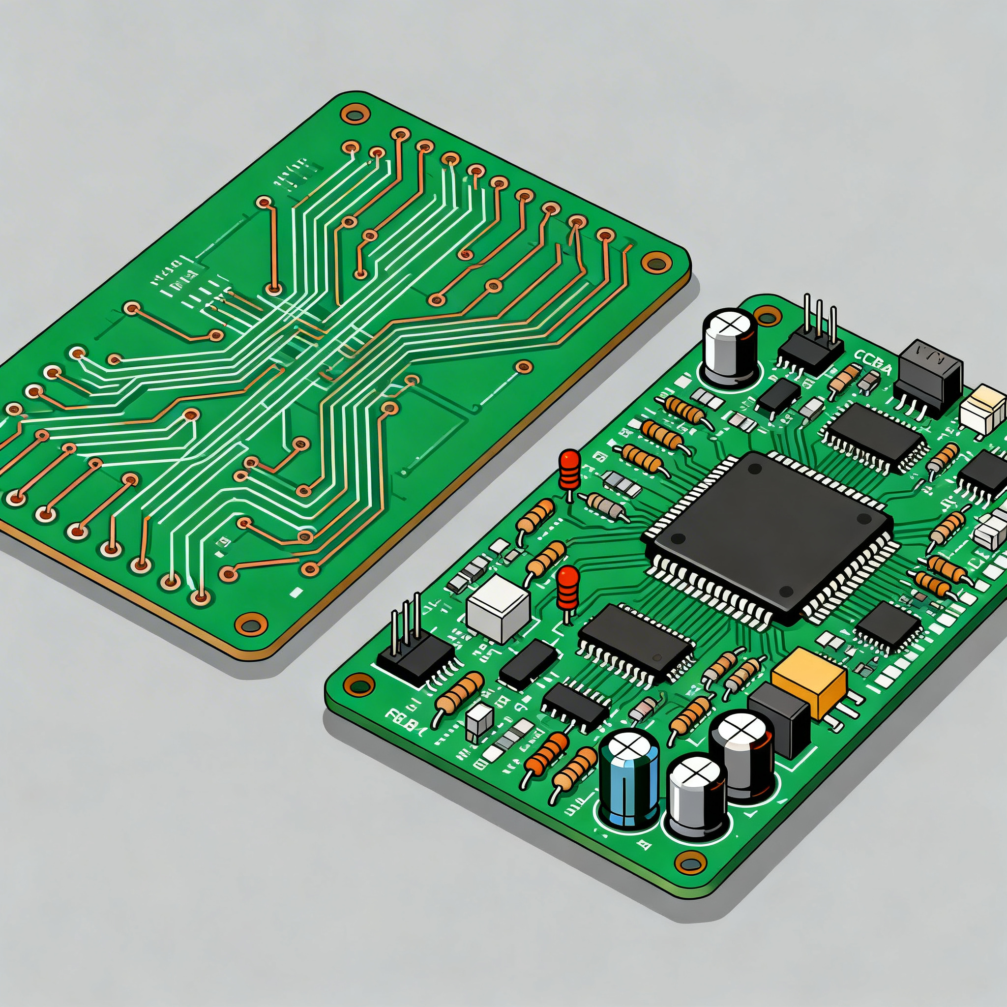
PCBs serve as the foundation for electronic components, providing mechanical support and electrical connections through conductive pathways. These boards are typically made from non-conductive substrates with embedded copper circuitry. On the other hand, PCBA refers to the assembly of components onto the PCB, transforming it into a functional electronic circuit. The process involves soldering various electronic components like resistors, capacitors, and integrated circuits onto the PCB. Understanding the technical aspects of both PCBs and PCBAs is essential for optimizing design and manufacturing processes, ensuring signal integrity, and achieving cost-effective production.
Detailed Specifications
When designing PCBs, adhering to specific design rules is essential to ensure functionality and reliability. These specifications include trace width, spacing, via sizes, and clearances. Each parameter impacts the board's performance, manufacturability, and cost. Understanding these specifications allows engineers to make informed decisions, reducing the likelihood of errors during the manufacturing process.
| Design Parameter | Minimum Value | Optimal Value |
|---|---|---|
| Trace Width | 0.15 mm | 0.25 mm |
| Trace Spacing | 0.15 mm | 0.20 mm |
| Via Diameter | 0.30 mm | 0.50 mm |
| Via Hole Size | 0.15 mm | 0.25 mm |
| Pad Size | 0.40 mm | 0.60 mm |
| Clearance | 0.20 mm | 0.30 mm |
| Solder Mask Clearance | 0.05 mm | 0.10 mm |
| Silkscreen Line Width | 0.10 mm | 0.15 mm |
| Aspect Ratio | 0.6:1 | 1:1 |
| Minimum Annular Ring | 0.10 mm | 0.15 mm |
| Board Thickness | 1.0 mm | 1.6 mm |
| Copper Thickness | 0.018 mm | 0.035 mm |
Key Takeaways from the Specifications
The specifications outlined in the table are critical for ensuring the functional integrity and manufacturability of PCBs. Trace width and spacing are paramount in preventing crosstalk and maintaining signal integrity. Via sizes and clearances impact the board's ability to support various component densities and layer counts. Adhering to optimal values where possible can enhance the board's performance and reliability while reducing manufacturing costs. Engineers must balance these parameters based on the specific requirements of their projects, considering factors such as current carrying capacity and thermal management.
| Layer Configuration | Description | Applications |
|---|---|---|
| 2-Layer | Basic design with top and bottom layers for routing. | Simple circuits, low-cost applications. |
| 4-Layer | Includes two internal layers for power and ground planes. | Improved signal integrity, moderate complexity. |
| 6-Layer | Additional layers for routing and power distribution. | High-speed circuits, EMI reduction. |
| 8-Layer | Enhanced signal integrity with multiple ground and power planes. | Complex designs, RF applications. |
| 10-Layer | Optimized for high-density interconnects and advanced routing. | High-performance computing, telecommunications. |
| 12-Layer | Maximum routing flexibility with dedicated signal layers. | Advanced applications, aerospace, and defense. |
| Rigid-Flex | Combination of rigid and flexible layers for 3D designs. | Wearable technology, compact devices. |
| HDI | High-density interconnect with microvias for compact designs. | Smartphones, tablets, and advanced electronics. |
Practical Implications
The choice of layer stackup significantly influences the PCB's performance and application suitability. For instance, a 4-layer board offers improved signal integrity and is suitable for moderate complexity designs, while a 12-layer board provides extensive routing flexibility for advanced applications. Rigid-Flex and HDI stackups are ideal for compact and high-density designs, providing solutions for modern electronic devices like smartphones and wearables. Engineers must consider the specific requirements of their projects, including signal integrity, EMI reduction, and mechanical constraints, when selecting the appropriate stackup configuration.
| Material | Dielectric Constant (Dk) | Loss Tangent (Df) |
|---|---|---|
| FR-4 | 4.5 | 0.02 |
| Rogers 4350B | 3.48 | 0.0037 |
| Rogers 4003C | 3.55 | 0.0027 |
| Isola 370HR | 4.04 | 0.016 |
| Nelco N7000-2 | 3.7 | 0.015 |
| DuPont Pyralux | 3.4 | 0.002 |
| Arlon 85N | 3.5 | 0.004 |
| Panasonic Megtron 6 | 3.5 | 0.002 |
| Taconic RF-35 | 3.5 | 0.0018 |
| Ventec VT-47 | 4.2 | 0.018 |
Application Guidelines
The choice of materials for PCB manufacturing is crucial for meeting the performance requirements of electronic devices. FR-4 is a cost-effective and widely used material suitable for general applications, while Rogers materials are preferred for high-frequency applications due to their low loss tangent. Materials like DuPont Pyralux are ideal for flexible circuits, offering a low dielectric constant and superior flexibility. Engineers should evaluate the dielectric constant and loss tangent to ensure signal integrity and minimize signal loss, particularly in high-speed and RF applications. Selecting the right material can significantly impact the device's performance, reliability, and cost.
Design Considerations
Designing a PCB involves several critical considerations to ensure optimal performance and manufacturability. Signal integrity is a key factor, where trace impedance, crosstalk, and ground plane design must be carefully managed. High-speed designs require controlled impedance, which can be achieved by selecting appropriate trace widths, spacing, and stackup configurations. Thermal management is another crucial aspect, particularly for power-dense designs, where adequate copper thickness and thermal vias are necessary to dissipate heat effectively. Additionally, designers must consider manufacturability, ensuring that the board design complies with fabrication capabilities and assembly processes. This involves adhering to design rules, choosing suitable materials, and optimizing component placement for automated assembly.
Step-by-Step Implementation
Implementing a PCB design involves several steps, each critical to achieving a successful outcome:
- Define Requirements: Establish the project's electrical, mechanical, and environmental requirements, ensuring alignment with end-use applications.
- Schematic Design: Create a detailed schematic capturing all electrical connections and components, serving as the blueprint for the PCB layout.
- Component Selection: Choose components based on electrical specifications, availability, and cost, ensuring compatibility with the design requirements.
- PCB Layout: Arrange components on the board, route traces, and define power and ground planes, adhering to design rules for optimal performance.
- Design Rule Check (DRC): Validate the layout against design rules to identify and correct potential issues before manufacturing.
- Prototype Fabrication: Order prototype boards from a manufacturer, specifying material, layer count, and finish requirements.
- Assembly and Testing: Assemble components onto the prototype boards, conducting functional and performance tests to verify the design.
- Design Iteration: Refine the design based on test results, addressing any issues and optimizing for production scalability.
Common Issues & Solutions
Designing and manufacturing PCBs can present several challenges. Here are common issues and their solutions:
- Signal Integrity Issues: Use controlled impedance traces and adequate spacing to minimize crosstalk and signal degradation.
- Thermal Management: Incorporate thermal vias and heatsinks to dissipate heat effectively, preventing component overheating.
- Manufacturability Errors: Perform DRC checks and collaborate with manufacturers to ensure the design is fabrication-ready.
- Component Placement: Optimize placement for automated assembly, reducing the risk of soldering defects and improving reliability.
- Material Selection: Choose materials that match the application's frequency and thermal requirements, ensuring performance and durability.
- Power Integrity: Design robust power distribution networks with adequate decoupling capacitors to maintain stable power delivery.
Applications & Use Cases
PCBs and PCBAs are integral to a wide range of electronic devices across various industries. In consumer electronics, they form the backbone of smartphones, tablets, and wearable devices, where compact and high-density designs are paramount. In automotive applications, PCBs are used in engine control units, infotainment systems, and safety features, requiring high reliability and thermal management. Aerospace and defense applications demand advanced PCBs with superior signal integrity and environmental resistance. In medical devices, PCBs enable compact and reliable solutions for diagnostic and monitoring equipment. Each application presents unique challenges and requirements, highlighting the importance of tailored PCB design and assembly.
Selection & Sourcing Guide
Selecting the right components and materials is crucial for successful PCB design and manufacturing. Engineers should consider factors like electrical performance, material properties, cost, and availability. Collaborating with reliable suppliers and manufacturers can streamline the sourcing process, ensuring quality and timely delivery. For sourcing components, visit IC Online, a comprehensive platform for electronic components and materials.
FAQ
Here are some frequently asked questions regarding PCBs and PCBAs:
- What is the difference between PCB and PCBA?
PCB refers to the bare board, while PCBA includes the board with assembled components. - How do I choose the right material for my PCB?
Consider factors like dielectric constant, loss tangent, and thermal properties based on application requirements. - What are the common design rules for PCB layout?
Key rules include trace width, spacing, via sizes, and clearances to ensure manufacturability and performance. - Why is signal integrity important in PCB design?
Signal integrity ensures reliable data transmission, minimizing errors and interference in high-speed designs. - How can I improve thermal management in my PCB?
Use thermal vias, heatsinks, and adequate copper thickness to dissipate heat effectively. - What is the role of a layer stackup in PCB design?
Layer stackup affects signal integrity, EMI performance, and routing flexibility, crucial for complex designs. - Can I use FR-4 material for high-frequency applications?
FR-4 is suitable for general applications but may not perform well at high frequencies; consider low-loss materials like Rogers. - What are the advantages of using HDI technology?
HDI technology offers compact designs with high-density interconnects, ideal for modern electronic devices. - How do I ensure my PCB design is manufacturable?
Collaborate with manufacturers, perform DRC checks, and adhere to design rules to ensure fabrication readiness. - What are the common causes of PCB failure?
PCB failures can result from poor design, inadequate thermal management, material selection, and manufacturing defects.
Conclusion
Understanding the differences between PCBs and PCBAs and the critical considerations in design and manufacturing is essential for engineers striving for optimal production. By adhering to design rules, selecting appropriate materials, and addressing signal integrity and thermal management, engineers can create reliable and high-performance electronic devices. This comprehensive guide serves as a valuable resource for navigating the complexities of PCB and PCBA design, ensuring successful outcomes in diverse applications.