pcba design rules
PCBA Design Rules: Circuit Topology, Component Calculations, Performance Analysis, and Design Trade-offs table { border-collapse: collapse; width: 100%; margin: 20px 0; } th, td { border: 1px solid #d...
Introduction
In the world of electronics, Printed Circuit Board Assembly (PCBA) is crucial for the functionality of electronic devices. As technology advances, the demand for compact, efficient, and reliable PCBAs increases. Understanding the design rules for PCBA is essential for engineers to ensure product performance and manufacturability. This article will delve into the intricacies of circuit topology, component calculations, performance analysis, and design trade-offs, providing a comprehensive guide for seasoned engineers and newcomers alike.
Technical Overview
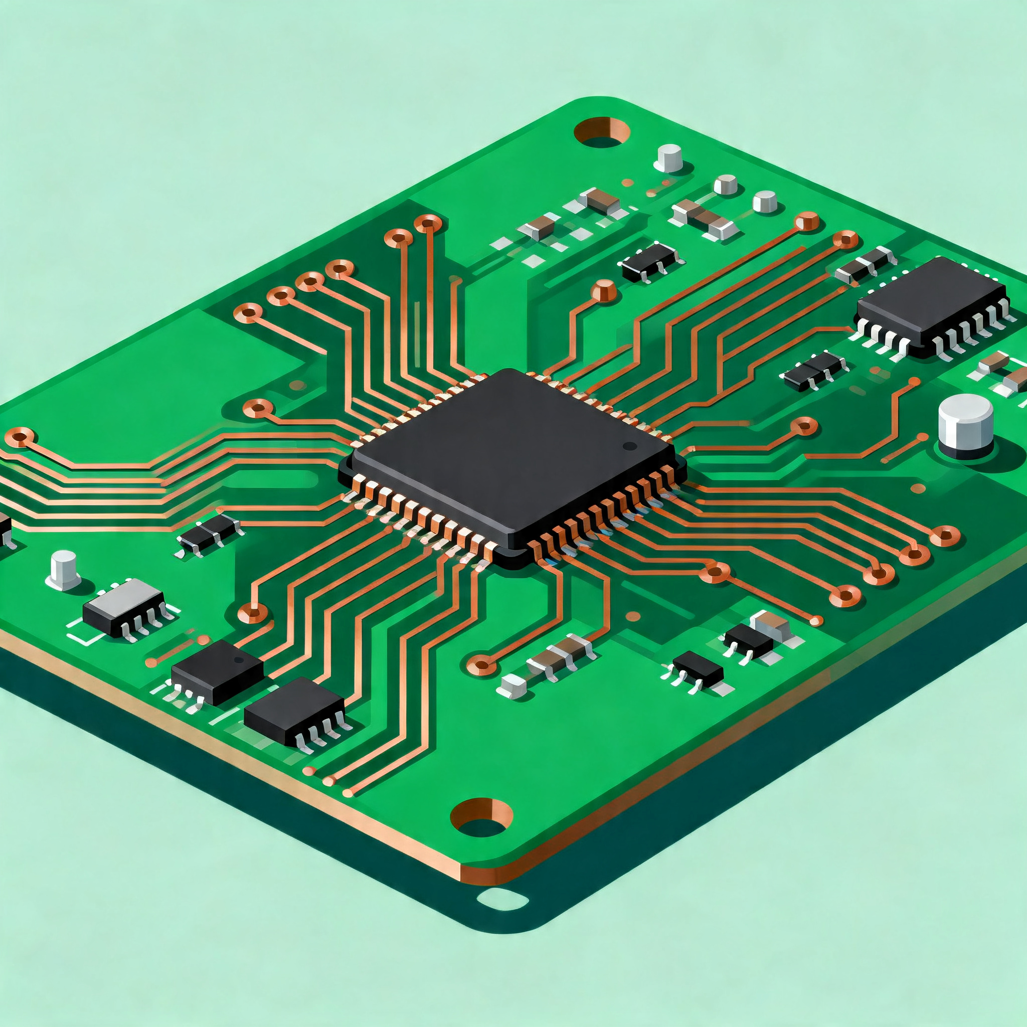
PCBA design involves several core concepts, including circuit topology, which defines the arrangement of various components on the board. The architecture of a PCBA is dictated by the design requirements, which may include considerations for signal integrity, thermal management, and power distribution. Key principles in PCBA design include minimizing electromagnetic interference (EMI), optimizing trace routing, and ensuring adequate grounding. Through meticulous planning and adherence to industry standards, such as those set by IPC, engineers can create PCBAs that meet both functional and regulatory requirements.
Detailed Specifications
When designing a PCBA, several specifications must be considered, including component values, trace widths, and spacing. These specifications ensure that the board can handle the required electrical loads and operate within its intended environment. Below is a detailed table outlining critical design parameters, including component calculations and formulas.
| Parameter | Value/Formula | Description |
|---|---|---|
| Resistance | 10kΩ | Standard resistor value for pull-up/down applications. |
| Capacitance | 100nF | Decoupling capacitor value for power supply stability. |
| Inductance | 10μH | Used in power supply filters to reduce ripple. |
| Trace Width | 0.25mm | Minimum width for signal traces to handle 1A current. |
| Trace Spacing | 0.15mm | Minimum spacing to prevent short circuits at 1kV. |
| Via Diameter | 0.5mm | Size for standard signal via to ensure manufacturability. |
| Power Rating | 0.25W | Standard power rating for resistors in low-power circuits. |
| Voltage Rating | 50V | Maximum voltage rating for ceramic capacitors. |
| Current Capacity | 1A/mm | Standard current capacity per mm of trace width. |
| Frequency | 1MHz | Typical operating frequency for general-purpose circuits. |
| Thermal Resistance | 100°C/W | Thermal resistance for standard SMD packages. |
Key Takeaways from the Specifications
The design parameters outlined above are crucial for ensuring that a PCBA can meet its performance and reliability requirements. The choice of component values, such as resistance and capacitance, directly impacts the circuit's functionality and stability. Trace width and spacing are essential for preventing overheating and ensuring signal integrity. By adhering to these specifications, engineers can design PCBAs that are not only functional but also manufacturable and cost-effective.
Performance Analysis
Analyzing the performance of a PCBA involves evaluating parameters such as gain, bandwidth, noise, and power consumption. These factors determine how well the board will perform in its intended application. The table below provides a detailed analysis of these performance metrics.
| Metric | Value | Significance |
|---|---|---|
| Gain | 20dB | Amplification level for signal processing circuits. |
| Bandwidth | 2GHz | Frequency range over which the circuit operates effectively. |
| Noise Figure | 3dB | Measure of noise introduced by the circuit components. |
| Power Consumption | 500mW | Total power used by the board under normal operation. |
| Signal-to-Noise Ratio (SNR) | 60dB | Ratio of signal power to noise power. |
| Harmonic Distortion | 0.05% | Measure of signal distortion due to non-linear elements. |
| Rise Time | 5ns | Time taken for a signal to transition from low to high. |
| Input Impedance | 50Ω | Standard impedance for RF circuits. |
| Output Impedance | 10Ω | Typical output impedance for signal transmission. |
Practical Implications
The performance metrics highlighted in the table are critical for assessing the suitability of a PCBA for specific applications. Gain and bandwidth are particularly important in communication and signal processing applications, where high signal fidelity is required. Noise figure and SNR are essential for ensuring that the circuit operates with minimal interference. By optimizing these parameters, engineers can enhance the overall performance and reliability of the PCBA.
Design Trade-offs
Designing a PCBA often involves making trade-offs between different configurations to achieve the desired balance between performance, cost, and manufacturability. The following table outlines some common design trade-offs encountered in PCBA design.
| Configuration | Pros | Cons |
|---|---|---|
| High-Density Interconnect (HDI) | Increased circuit density | Higher manufacturing cost |
| Thick Copper PCBs | Better power handling | Increased weight and cost |
| Single-Layer PCB | Lower cost | Limited routing space |
| Multi-Layer PCB | Greater routing flexibility | Complex manufacturing process |
| Flexible PCBs | Adaptability to complex shapes | Higher material cost |
| Surface Mount Technology (SMT) | Compact design | Requires precise placement equipment |
| Through-Hole Technology | Stronger mechanical bond | Larger board space required |
| Lead-Free Solder | Environmentally friendly | Higher melting temperature |
Application Guidelines
The design trade-offs presented highlight the need to carefully consider the specific requirements of each project. While HDI and multi-layer PCBs offer higher performance and flexibility, they come at a higher cost. Conversely, simpler designs like single-layer PCBs may be more cost-effective but offer limited functionality. Understanding these trade-offs allows engineers to make informed decisions that align with project goals and budget constraints.
Design Considerations
Designing a PCBA requires a careful balance of several factors to ensure optimal performance and reliability. Engineers must consider electrical, thermal, and mechanical aspects, adhering to industry standards such as IPC-2221 for general design requirements and IPC-A-610 for assembly and workmanship. Key considerations include trace routing to minimize EMI, selecting appropriate materials for thermal management, and ensuring adequate component spacing to prevent short circuits. Additionally, the choice of assembly technology, whether SMT or through-hole, can impact the manufacturability and cost of the board. By meticulously planning each aspect of the design, engineers can create PCBAs that meet both functional and regulatory requirements.
Step-by-Step Implementation
Designing a PCBA can be broken down into several key steps:
- Define Requirements: Clearly outline the electrical, mechanical, and environmental requirements for the PCBA.
- Component Selection: Choose components that meet the specifications and are readily available from suppliers.
- Schematic Design: Create a detailed schematic diagram that represents the electrical connections and components.
- PCB Layout: Use ECAD software to design the physical layout, ensuring optimal trace routing and component placement.
- Design Rule Check (DRC): Perform DRC to ensure the layout adheres to design standards and manufacturing constraints.
- Prototype Fabrication: Manufacture a prototype to test the design under real-world conditions.
- Testing and Validation: Conduct thorough testing to verify that the PCBA meets all performance and reliability criteria.
- Production Release: Once validated, prepare the design for mass production, including generating manufacturing files and documentation.
Common Issues & Solutions
During the design and manufacturing of PCBAs, several common issues can arise:
- Signal Integrity Problems: Ensure proper trace routing and impedance matching to prevent signal degradation.
- Thermal Management Challenges: Use thermal vias and heat sinks to dissipate heat effectively.
- Component Placement Errors: Follow assembly guidelines to ensure correct orientation and spacing.
- Manufacturing Defects: Work closely with the manufacturer to address issues such as solder bridging and misalignment.
- EMI/EMC Compliance: Implement shielding and filtering techniques to minimize electromagnetic interference.
- Supply Chain Disruptions: Maintain a list of alternate suppliers to mitigate component shortages.
Applications & Use Cases
PCBAs are utilized in a wide range of applications, from consumer electronics to industrial automation. In the automotive industry, they are used for engine control units and infotainment systems. In telecommunications, PCBAs form the backbone of network infrastructure. Medical devices rely on PCBAs for monitoring and diagnostic equipment. Each application presents unique challenges, requiring tailored design approaches to meet specific performance and regulatory requirements.
Selection & Sourcing Guide
When selecting components and sourcing materials for a PCBA, it's crucial to consider factors such as availability, cost, and compliance with industry standards. Online resources like IC Online provide comprehensive databases of components and suppliers, helping engineers make informed decisions and streamline the sourcing process.
FAQ
Here are some frequently asked questions regarding PCBA design:
- What is the importance of trace width in PCB design? Trace width determines the current-carrying capacity and affects signal integrity.
- How do I select the right components for my PCBA? Consider electrical specifications, availability, and cost when selecting components.
- What are the benefits of using multi-layer PCBs? Multi-layer PCBs offer greater routing flexibility and improved performance.
- How can I minimize EMI in my design? Use proper grounding, shielding, and filtering techniques to reduce EMI.
- What is the role of thermal management in PCBA design? Effective thermal management prevents overheating and ensures reliability.
- How do I ensure my design is manufacturable? Follow design rules and work closely with the manufacturer to address potential issues.
- What are the common causes of manufacturing defects? Misalignment, solder bridging, and component placement errors are common causes.
- How can I address supply chain disruptions? Maintain relationships with multiple suppliers and have alternate components ready.
- What is the significance of IPC standards? IPC standards ensure quality, reliability, and manufacturability of PCBAs.
- How do I test my PCBA design? Use simulation and prototyping to validate performance and identify potential issues.
Conclusion
Designing a PCBA requires a comprehensive understanding of circuit topology, component calculations, performance analysis, and design trade-offs. By adhering to industry standards and leveraging the knowledge of experienced engineers, PCBAs can be crafted to meet the diverse needs of modern electronics. Whether for consumer, industrial, or medical applications, a well-designed PCBA is integral to the success and reliability of electronic devices.